Introduction
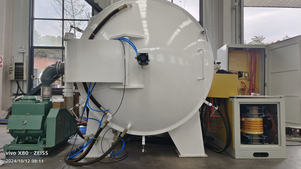
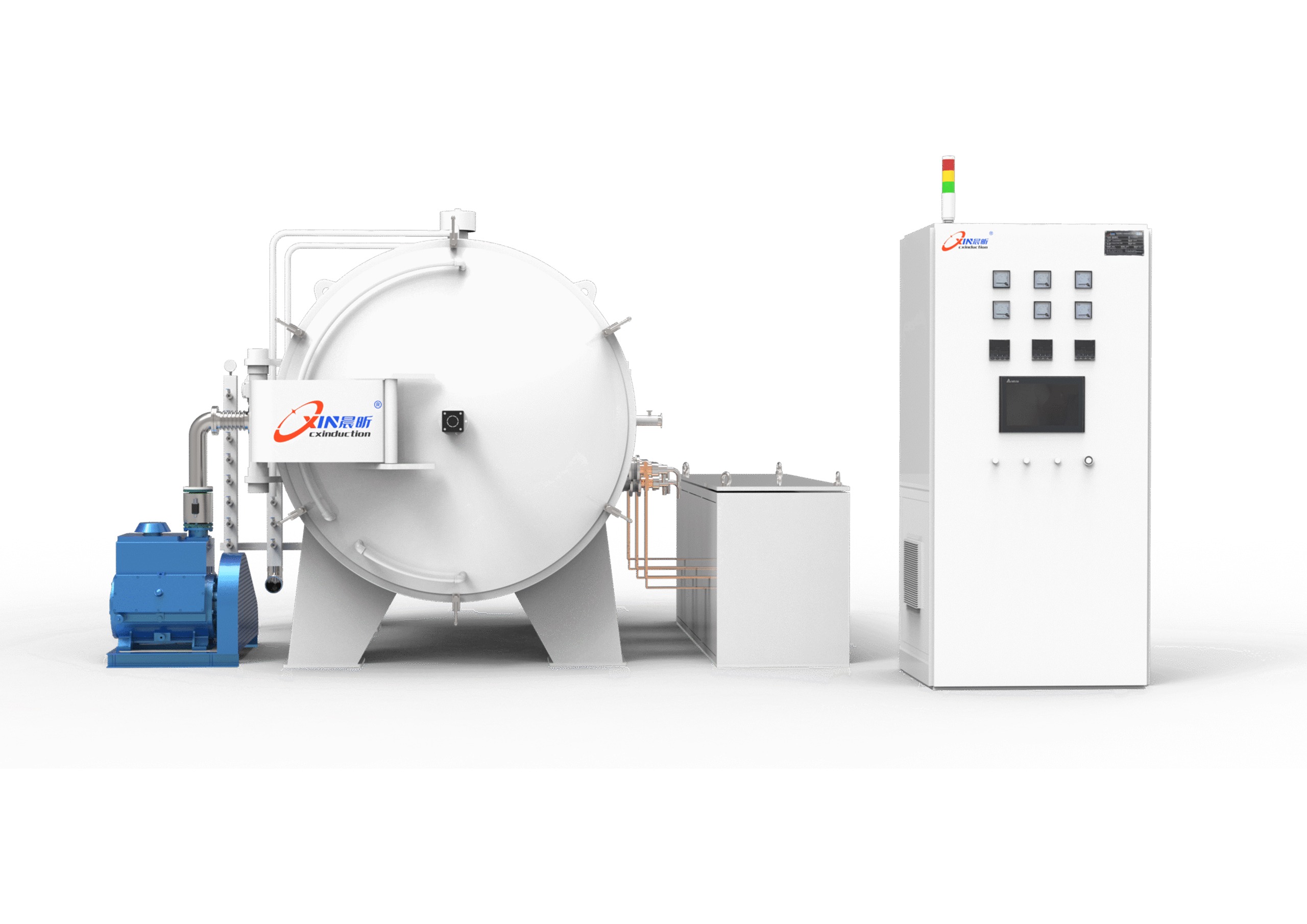
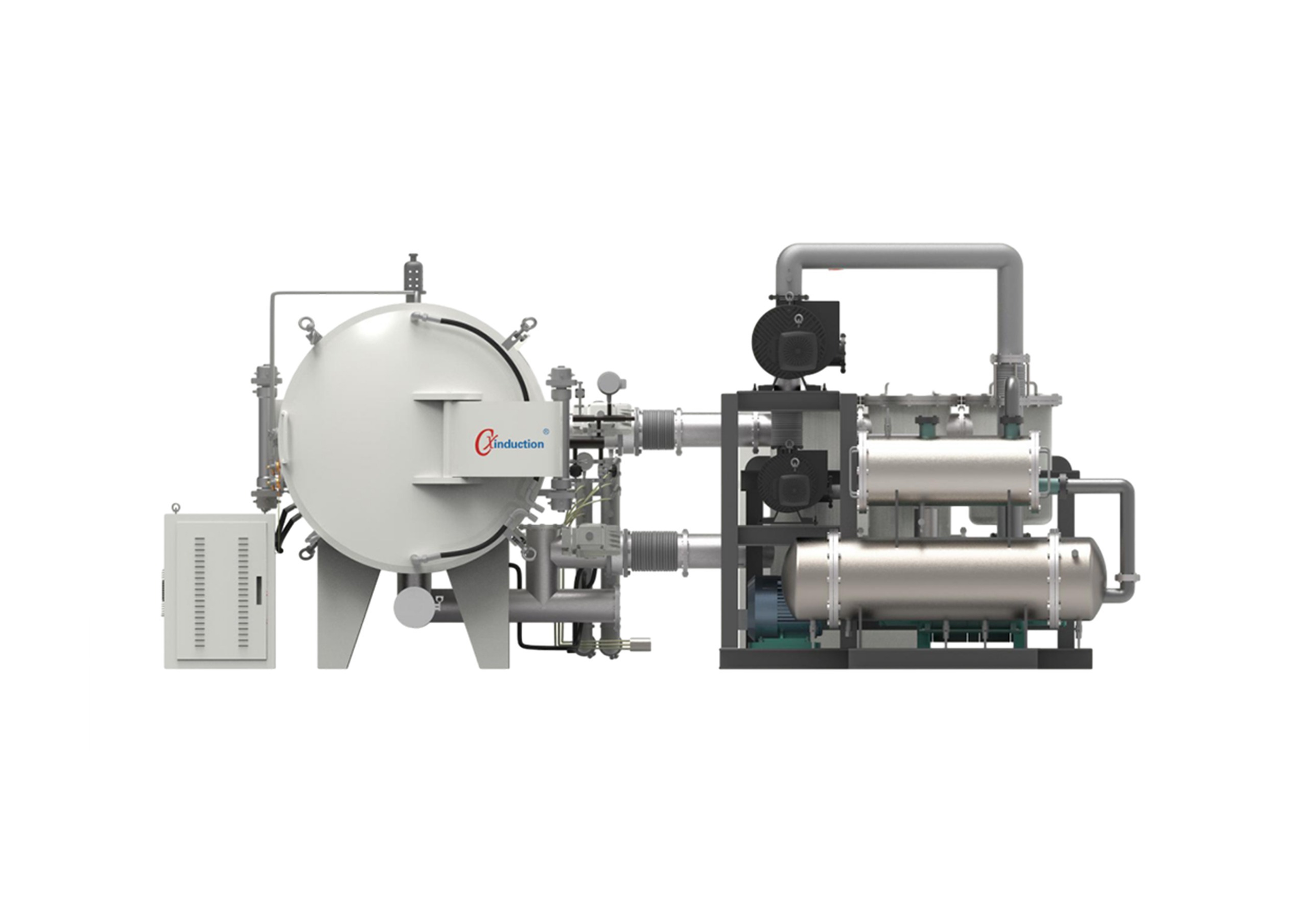
Silicon carbide (SiC) epitaxial substrates have emerged as a critical material in high-power, high-frequency, and high-temperature applications, driving advancements in electric vehicles (EVs), renewable energy, industrial equipment, and consumer electronics. The superior properties of SiC, including wide bandgap, high thermal conductivity, and exceptional breakdown voltage, make it indispensable for next-generation semiconductor devices. To produce high-quality SiC epitaxial layers, chemical vapor deposition (CVD) is the preferred method, with Cxinduction’s CVD furnace standing out due to its precision engineering, multi-gas uniform distribution, accurate flow control, and constant-pressure mode. However, the sintering process demands strict attention to critical parameters to ensure optimal material performance.

Electric Vehicles & Renewable Energy
SiC-based power devices significantly enhance EV efficiency by reducing energy loss in inverters and onboard chargers. Compared to traditional silicon, SiC enables faster switching, higher voltage tolerance, and improved thermal management, extending driving range. In solar and wind energy systems, SiC devices optimize power conversion, minimizing energy waste.
Industrial & Consumer Electronics
Industrial motor drives, UPS systems, and high-voltage converters benefit from SiC’s robustness in harsh environments. Meanwhile, consumer electronics leverage SiC for compact, high-efficiency power supplies (e.g., fast chargers).
Producing defect-free SiC epitaxial layers requires precise control over gas flow, temperature, and pressure. Cxinduction’s CVD system excels in:
Multi-Gas Uniform Distribution: Ensures homogeneous precursor (e.g., argon, acetylene) delivery across the substrate, critical for uniform film thickness and doping.
High-Accuracy Flow Control: Mass flow controllers (MFCs) maintain stoichiometric ratios, preventing Si/C imbalance that causes crystallographic defects.
Constant-Pressure Mode: Stabilizes the reaction chamber, minimizing turbulence and ensuring consistent deposition rates.
High-Temperature Capability: Reaches 1600℃+ for high-quality crystalline growth, with minimal thermal gradient-induced stress.
Smart Process Automation: After setting temp ramp and parameter, system work automatically.
While CVD is pivotal, sintering—a step often used in SiC ceramic production—requires careful handling to avoid defects:
A.Temperature Ramp Rate
Challenge: Rapid heating induces thermal stress, leading to cracks.
Solution: Gradual temperature increase (e.g., 5–10℃/min) ensures uniform expansion.
B.Gas Atmosphere Control
Inert vs. Reactive Gases: Argon/N2 atmospheres prevent oxidation, while acetylene requires leak-proof safety measures.
Impurity Avoidance: Trace O2 or H2O degrades SiC purity; gas filters and vacuum pre-purging are essential.
C.Pressure Management
CVD Integration: In-situ pressure control during deposition prevents flaking or uneven adhesion.
D.Substrate Preparation
Surface Polishing: Submicron surface roughness minimizes nucleation defects.
Off-Axis Cutting: 4° off-axis SiC wafers promote step-flow epitaxy, reducing screw dislocations.
E.Contamination Prevention
Crucible Material: High-purity graphite or TaC-coated crucibles resist SiC reaction.
Particulate Control: Cleanroom (Class 100 or better) handling avoids embedded particles.
As demand for SiC devices grows, advancements in multi-wafer CVD systems and smart process optimization (e.g., real-time gas flow adjustment) will further improve yield. Cxinduction’s technology, with its emphasis on uniformity and stability, is poised to support this expansion.
5.Conclusion
SiC epitaxial substrates are revolutionizing power electronics, enabled by precision tools like Cxinduction’s CVD furnace. By adhering to stringent sintering protocols—controlled heating, gas purity, pressure stability, and contamination mitigation—manufacturers can harness SiC’s full potential. The synergy of advanced equipment and process expertise will continue to propel innovations across EVs, green energy, and beyond.

Advanced CVD Solutions for SiC Semiconductor Manufacturing presents a 1600℃ Multi-Atmosphere CVD Furnace specifically engineered

Precision CVD System for High-Quality Graphene Production presents a 1600℃ Multi-Atmosphere CVD Furnace engineered for reliable